S100 Computers

HomeS-100 Boards HistoryNew BoardsSoftwareBoards For Sale
ForumOther Web SitesNewsIndex  
  
An S-100 Bus 8 Bit VGA Video Board.   
  VGA Board (Final)
 
Introduction
Many S-100 board manufactures had their own Video boards.  Most initially were character based "video TTY's". The very early ones were restricted to 64 characters/line (for example the SSM board) but soon 80 characters per line became common.  A good example is the SD Systems 8024 Board.

As time went on, boards started to get more sophisticated and began to offer fairly high resolution graphics capabilities.  A good example of this would be the Matrox ALT512 board which offered color graphics at a 512 X 256 resolution. There were even a few of higher resolution.  The NEC 7220 based video controller boards for example, which brought video display graphics to a new level. That chip was the NVIDEA chip of its day back in the early 1980's.

Once the IBM PC appeared on the scene video hardware compatibility with it became key.   There were a few S-100 bus attempts to make equivalent cards. The Lomas "Color Magic" IBM-PC Color Graphics Adaptor (CGA) look-alike probably being the most successful.  However with the phasing out of the S-100 bus in the late 1980's, no higher resolution S-100 video boards were ever produced. 

On the IBM-PC side of things (and its clones), video boards of increasing resolution appeared, eventually culminating in "VGA" boards. At the same time a very long list of "all in one" PC video chips were developed. The firm Chips and Technologies was the first company (outside of IBM) to deliver a compatible VGA chipset, the 82C451. This market was then entered into by companies such as Trident Microsystems, Western Digital, Cirrus Logic, Oak Technologies, and others, until it was saturated.  None of them exist today, nevertheless they started a whole industry of powerful all in one video chips.   With one chip,  a little DRAM and a ROM a complete video board could be constructed with outstanding capabilities.

With the recent of our introduction of our 8088 based S-100 boards and MS-DOS based operating system there is a clear need for a good high resolution VGA style video board.  The specifications of a VGA board is beyond the capability of discrete 74LSxx based TTL chips.   This is the job of a dedicated "Video Controller Chip".  What chip should one use ? There are a number of candidates.  In the end I settled for the TVGA9000 made by Trident Microsystems .  Major points in its favor were SVGA resolution, an onboard DAC, an excellent manual describing the chip and reasonable availability.  The only catch is that it only exists in a 164 pin surface mount version -- as do all these video chips.

TVGA9000 General Information
The TVGA9000 according to Trident Microsystems is a versatile and full-featured single-chip solution for VGA (Video Graphics Array) systems. The chip provides register-level compatibility, enhanced graphics and text modes, support for 256Kx4 DRAMs, plasma display control; and support for analog VGA, , EGA, CGA, and MDA monitors. The chip provides register-level compatibility with standard IBM VGA modes and backward compatibility with EGA, CGA, MDA. and Hercules modes. The enhanced graphic and text modes provide high-resolution displays in 4, 16, and 256 colors. Support for 256x4 DRAMs saves board space and provides cost savings.

Display support for analog VGA. digital VGA, plasma, EGA, CGA, MDA. and Hercules monitors assures that the TVGA9000 board solution may be used with virtually any monitor on the market.

Compatibility
The TVGA9000 supports both the PC/AT bus and the PS/2 Micro Channel bus. The TVGA9000 is fully compatible with all standard IBM VGA modes and EGA. CGA. MDA, and Hercules modes, and allows the following: Use of all application software for VGA. EGA, CGA, MDA, and Hercules modes Emulation of EGA, CGA, MDA. and Hercules modes on a VGA monitor.

Text Modes
  
 Extended Graphics and Text Modes Extended graphics modes supported by the TVGA9000 include the following:
    64Ox400, 640x480 and 800x600 in 256 colors from a palette of 256K116M.
    800x600 and 1024x768 (interlaced or non-interlaced) in 16 colors from a palette of 256K116M.
    1024x768 in4 colors from a palette of 256K/16M.
    Extended text modes offer 132-column text with 25, 30,43. and 60 rows.
  
   
  Trident Chip
    
This chip is clearly an almost self contained XVGA board.  The only major support chips are a 27C256 BIOS EPROM and four 4X256K DRAM chips.   The datasheet for the chip can be obtained here.

I used an IBM PC ISA board designed Sergey Kiselev Sergey's ISA Super VGA board with our ISA to S100 bus adaptor board to test if I could use this board in an S100 bus system. 

Using Sergey's ISA board in our ISA to S100 bus converter I could test and fine tune a future fully dedicated S100 bus XVGA board.   Simple and all as this looked it took several prototype boards to get a reliable one.  The breakthrough came when I switched over to using GAL's as the core part of the S100 bus interface circuit.  If you are not familiar with GALs please read the summary description here. You should also read the description of the ISA to S100 bus converter board as most of the circuit and GAL's are based on this board.

There is one major limitation with this S100 bus XVGA board,  it will only work with our 8088 CPU board. With that board as best I can tell,  it is rock solid running MSDOS with an S100  bus clock speed (PHI) of 8 MHz (i.e. a 24 MHz Oscillator on the board).  It will NOT work with our current 16 bit CPU's ( the 8086, 80286 or 80386).  The reason for this is due to the fact that these VGA chips (at least for the Cirrus & Trident chips),  require the CPU to be able to send 16 bit data as two back to back 8 bit bytes.   The chips actually have dedicated lines (MCS16* & IOCS16*) to flag the CPU to let it know it is capable of a 16 bit transfer.  However I found out the hard way, that these chips do not always exercise this option -- particular during initialization.  On our ISA converter board I played around with the circuit to sequentially send two 8 bit bytes using  Sergey's ISA Super VGA board.  I could not find a reliable solution.  The best effects were sensitive to the bus CPU speed and failed altogether at high MHz speeds.   Perhaps somebody else may have better luck programming the GAL's on that board.

The fundamental problem was that these VGA chips can, and do, pull wait states on the bus at impossible to determine times (particularly during screen scrolls).   The length of the wait states is highly variable.   I concluded the only way to solve this is to redo the CPU boards themselves so that if the 16 bit CPU board does not get a SIXTN*  acknowledge from a sXTRQ*, it proceeds to send two back to back 8 bit bytes.  This was actually part of the IEEE-696 specification.  However most manufactures at the time (an also in our cases),  ignored this and simply supplied 16 bit capable RAM and/or IO boards.  The only documented circuit I could find for an 8+8 bit 8086 CPU S100 board was the (excellent) one described for the TecMar 8086 board.

The good news is that the 80486 CPU has the ability to on the fly  send 8, 16 or 32 bit data depending on the chips on the receiving end.  The other good news is that this XVGA board can send and receive 16 bit data. The VGA chip itself has 16 bit data pins so such a board should work at full speed with such a 80486 CPU.  Most of the time transfers will be 16 bits but initialization and ROM access will be 8 bits -- just as in the IBM-AT box! 
As to building the above board. Its actually a fairly simple board.  However in some places the traces are quite close. There are situations for the bottom row of IC' s where two traces run between pins.  Take care not to add too much solder to the IC pins.  (That error cost me a day!).
 
Second, the Trident chip comes only in a surface mount format.  I found that these chips are fairly intolerant to overheating the pins (unlike for example our recent Static RAM SMD chips).    The trick is to paint the board area with solder flux, then place a layer of solder on the pads. The flux makes sure they do not cross bridge.  Use a fine solder wire (0.15").  The place the chip on the board. Aligned carefully, solder one corner, the opposite corner.   Using a fine tip,  touch the solder on the pad and draw it towards the end of the chip pin.  When done with a fine blade touch each pin to make sure it does not move.  With this method it is quite easy to attach the chip to the board.  Clean off the excess flux with flux remover spray.

To ease the tension/risk of attaching a chip to this board I have incorporated an intermediate step in the build process where you can attach Sergey's ISA Super VGA board to an 8 bit ISA connector on the board.  This allows you to debug/test your S100 interface before taking the plunge of attaching a Trident chip to the board directly.   Here are two picture of the board with this intermediate step.
Final Board2
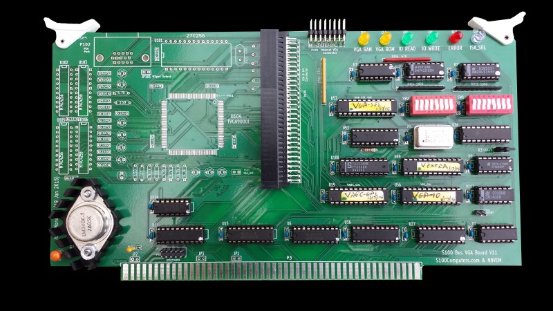
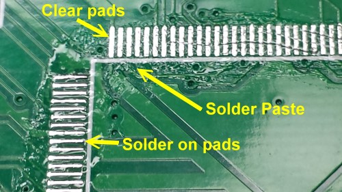
                                               VGA board before adding ISA Board
Final Board 3
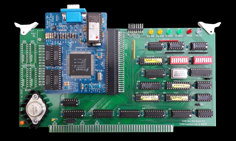
                                          VGA Board with ISA VGA board attached 
   

The nice thing about this approach is you can be sure your VGA chip/circuit/components are fine by first testing them in an old IBM-PC compatible box.  The circuit on the S100 board itself is exactly the same as that of Sergey's. The board circuit feeds directly from the ISA pins on the S100 board.  Remember however that once you attach the VGA chip to your S100 board directly you cannot use  Sergey's ISA Super VGA board


Here is a picture of the final prototype board with the Trident chip soldered directly to the board:-
   Final Board


Here is a short video describing the board and showing it running in my test system. 


The GAL's
There are four simple GALs on this board. The first two are dedicated to providing I/O port  and memory "holes" in the S100 bus address space to communicate with the VGA chip.
 
VGA_IO sets aside all the possible I/O ports the chip will need:-

/VGA_PORTS =  /SA15 * /SA14 * /SA13 * /SA12 * /SA11 * /SA10 * /SA9 * SA8 ;Port 102H,103H OUT
            * /SA7 * /SA6 * /SA5 * /SA4 * /SA3 * /SA2 * SA1
            * bsOUT * /bsINTA

          +   /SA15 * /SA14 * /SA13 * /SA12 * /SA11 * /SA10 * /SA9 * SA8 ;Port 102H,,103H IN
            * /SA7 * /SA6 * /SA5 * /SA4 * /SA3 * /SA2 * SA1
            *  bsINP * /bsINTA

          +   /SA15 * /SA14 * /SA13 * /SA12 * /SA11 * /SA10 * SA9 * SA8 ;Port 03BxH OUT
            *  SA7 * /SA6 * SA5 * SA4
            *  bsOUT * /bsINTA

          +   /SA15 * /SA14 * /SA13 * /SA12 * /SA11 * /SA10 * SA9 * SA8 ;Port 03BxH IN
            *  SA7 * /SA6 * SA5 * SA4
            *  bsINP * /bsINTA

          +   /SA15 * /SA14 * /SA13 * /SA12 * /SA11 * /SA10 * SA9 * SA8 ;Port 03CxH - 03DXH OUT
            *  SA7 * SA6 * /SA5
            *  bsOUT * /bsINTA

          +   /SA15 * /SA14 * /SA13 * /SA12 * /SA11 * /SA10 * SA9 * SA8 ;Port 03CxH - 03DXH IN
            *  SA7 * SA6 * /SA5
            *  bsINP * /bsINTA

VGA_SEL sets aside all the possible RAM address areas the chip will need for display memory.  These are phantomed out of the S100 bus address space:-

                                                                 ;Read/Write RAM 0BxxxxH & 0AxxxxH
/VGA_RAM   = LA19 * /LA18 * LA17 *  SA16 * /LA23 * /LA22 * /LA21 * /LA20 
           + LA19 * /LA18 * LA17 * /SA16 
* /LA23 * /LA22 * /LA21 * /LA20  

                                                                 ;Read ROM C0000 to CxxxxH RAM (Not write)
/VGA_ROM   = LA19 * LA18 * /LA17 * /SA16
* /bsMWRT  * /LA23 * /LA22 * /LA21 * /LA20    

ISA_SEL    = /VGA_RAM + /VGA_ROM + /VGA_PORTS         ;The Main Board address selection line

/ISA_PORT_READ    =   /VGA_PORTS * bsINP              ;For read VGA Ports LED
/ISA_PORT_WRITE   =   /VGA_PORTS * bsOUT              ;For Write VGA Ports LED
/ISA_ROM_READ     =   /VGA_ROM * bsMEMR               ;For read VGA ROM LED


VABC_GAL sets the OE* and direction of the S100 bus data buffers U26, U27  & U108.  (U108 is not currently used)

/A_SIGNAL     =  bsMEMR * ISA_SEL * bpDBIN           ;Enable CPU READ 8 bits from U26
              + bsINP * ISA_SEL * bpDBIN

/DIRECTION_1  = ISA_SEL * bpDBIN                     ; * bsXTRQ ;LOW, READ 8 bits, U26, Set pin 1 direction B -> A


/B_SIGNAL     =  bsMWRT * ISA_SEL * /bpWR            ;* bsXTRQ ;Enable CPU WRITE 8 bits via U27
               + bsOUT * ISA_SEL * /bpWR


DIRECTION_2   = ISA_SEL * /bpWR                      ;HIGH, WRITE 8 bits, U27, Set pin 1 direction A -> B


/C_SIGNAL =    bsMWRT * ISA_SEL * /bpWR * /bsXTRQ * /MEMCS16       ;WRITE 16 bits via U27 (Not currently used)
             + bsOUT * ISA_SEL * /bpWR * /bsXTRQ * /IOCS16
             + bsMEMR * ISA_SEL * bpDBIN * /bsXTRQ * /MEMCS16      ;READ 16 bits via U27 (Not currently used)
             + bsINP * ISA_SEL * bpDBIN * /bsXTRQ * /IOCS16


/ISA_SEL_LED = ISA_SEL * bsXTRQ                      ;Flash LED indicating a board request
/ERR_LED = ISA_SEL * /bsXTRQ                         ;Flash LED indicating board can not handle 16 bits

/SIXTN@ =  ISA_SEL * /IOCS16                         ;Indicating to S100 bus Trident chip can handle 16 bits
         + ISA_SEL * /MEMCS16


VEXTRA  This GAL provides the four memory/IO read/write signals:

/ISA_MEMW =    bsMWRT * ISA_SEL * /bpWR

/ISA_MEMR =    bsMEMR * ISA_SEL * bpDBIN

/ISA_IOW  =    bsOUT * ISA_SEL * /bpWR

/ISA_IOR  =    bsINP * ISA_SEL * bpDBIN

As you can see these are very simple GAL's, nevertheless they save a considerable number of 74LSxx chips.  There are a number of GAL programmers available these days. I have been using the Wellon V290 

Step By Step Building the VGA Video Board.
As always, first examine the bare board carefully for scratches or damaged traces, use a magnifying glass if need be. There was a minor silkscreen labeling problem on the board. Resistors R104, R108 and R 103 were not labeled on the board. They are to the left of the TVGA chip. A printout of all components on the board will be sent with the board to users.

I find it useful to carefully slide a file at 45 degrees along the edges (front & back) of the S100 connector at the bottom of the board for easier insertion of the board  into the bus. Carefully, just one or two strokes.
   
Next solder in all the required IC sockets, resistors, resistor arrays, capacitors, jumpers, the 14.318 MHz crystal and the voltage regulator. 

If you are going to first run the video board with Sergey's ISA Super VGA board do not solder in any components left of the ISA bus socket.  If you add a right angled ISA connector you will not be able to fit in the actual ISA video board. 

If you only intend the ISA video board to be a temporary testing step (the normal arrangement), you may want to consider using the much more common straight pinned ISA connector and run the ISA video board at right angles in an S100 bus extender board.   Alternatively you can use two single row female 0.1" headers (as I did here) and temporally put the straight or right angled ISA socket in them.  Lastly you can make your own right angled ISA socket by using a straight pinned socket and soldering to the pins two rows or right angled header pins.


Be sure you put the resistor array in with the correct orientation of pin 1. Check their values before soldering (they are difficult to remove). 
When you
add the LED's be sure they work and are in the correct orientation by temporally grounding the appropriate pins on the GAL socket at U757.

  
For this board there are no traces under the LM323K 5V regulator heat sink so a mica insulator is not required but always a good thing to add.  Be sure to test your TO-3 regulator for 5 volts before adding it to the board, there are many out of specs out there -- particular on eBay. Anchor Electronics has reliable ones I know - I use them.
  
For prototype boards I generally use "double swipe" IC sockets. For a critical board like this I prefer to use "Machine Tooled" IC sockets.  However they are more expensive and you have to be particularly careful not to bend the IC pins. 

This is a relatively simple board with few IC's on the right hand side. That said, the traces on the board are very fine, often with two or three traces running between the IC pins. Use care in soldering, use less solder rather than more.

After checking the voltage at Vcc on each IC chip socket is between 4.95 and 5.05 Volts insert all the IC's. as well as the 14.318 Oscillator.  For an 24MHz driven 8088 CPU board start with 4 wait states. So close the 4 right most switches on the dip switch sockets SW1 and SW2.

You now need to program 4 GALS. The source and .JED files are given below.   These are very simple PALASM programs and you should have no problem "burning" the 22V10 GALs.  If you get stuck I will burn GAL's for you if you send them to me with a self contained return package.
 
Next insert the board in your system and transfer control to you 8088 CPU monitor (Z80 "O" command).  If you do a memory map the ISA_SEL, VGA_RAM and VGA_ROM LED's should briefly flicker when you get to C0000H.
 
Inputting or outputting  any port in the range 102-103H, 46E8 - 46E9H, 3B0-3DFH should cause pin 15 of U56 to pulse.

At this point you are ready to insert the ISA VGA board.  With the 8088 monitor the VGA ROM should appear as "p" in the C0000H - C7FFFFH range.   Next check the first two bytes of the ROM read as "
55 AA".  If not, you must determine the problem. The board will not boot up in MSDOS without a valid ROM.

If the above is OK, hook-up a VGA cable to your ISA boards connector and boot MSDOS.   The system should automatically (after some time) display the MSDOS signon etc.  Note you may need to enter an initial keyboard CR to complete the signon.

If the above works, you are half way there.  Next comes the tricky step of adding the Trident SMD chip.   Everybody has their own favorite way of mounting these large SMD chips.   I found out the hard way that these Trident chips are more sensitive than most to pin overheating!   I find the best way to solder them to the board is to apply plenty of solder flux paste to the pads, then with a fine tipped solder tip run solder along all the pads. It will bulge up on the pads themselves with no bridges.  Here is a picture:-
            
  Solder pads
 
Next place the Trident chip on the pads. Be sure pin 1 is at the top right hand corner (unlike all the other chips on the board).  Carefully aligned the chip so all pins are aligned. Then solder (only) pin 1 by lightly pressing down on the chips pin.  Next do the same for pin 81.  Very carefully look around the chip and be sure each pin is aligned up exactly with it's pad.  Use a sharp blade between pins to reposition a pin if necessary.   Then go around the chip by simply touching the boards solder pads at the end of each pin. The solder will quickly weak up under the pin.  No more than a half a second is required.  It actually becomes quite easy to do.  Afterwards spray the area with flux remover and inspect each pin under a magnifying glass/light by trying to move a pin with a blade edge. It should not move.

Next add the four DRAM sockets and chips.  Also add the actual VGA connector socket.   You then need to add the various support caps, chokes, and resistors for the Trident chip.  Also add the 40 MHz crystal.    Here is a picture of the final board:-
  VGA Final
   
There are a few jumpers on the board. Normally JP101 is closed and jumper K3 is position 1-2.   P105 is normally 1-2.

Most of the IC's use on this board are common 74LSxx chips available from numerous sources such a Jameco, Mouser & DigiKey.  Here in the San Francisco bay area I recommend Anchor Electronics. They take phone orders as well and are well stocked.    

Here are Jameco catalogue numbers of some components:-
14.3MHz Oscillator    #537799
22V10 GAL's    #39159
470 Ohm Resistor pack    #97869
1K Ohm Resistor pack    #78777
Dual Row jumper headers #67821
Single Row Jumpers (cut to size) #527654
Bypass capacitors  #25525  (Many, not included in BOM below)

The support caps and  chokes I got from Mouser
EMI filters  623-2743001112LF
Inductor (5.6uH)  542-78F5R6J-RC
Inductor (2.7 uH)  542-78F2R7-RC
Cap 0.10uF  810-FK28X7R1H104K
Cap 10uF    810-FK24X5R1C106K
Cap 100 pF  810-FK28C0G1H101J
Cap 470pF    810-FK28C0G1H471J

The TO-3 78H05 's are hard to find. You can also use the Jameco 3A LM323K's (#23667). Check your voltage before inserting the IC's as mentioned above. Anything between about 4.95V and 5.1V  should be OK.  Rick Bromagem has kindly supplied a BOM, see bottom of this page.

The right angled ISA 62 pin socket is not that common.  Mouser has them #571-5532600-4 .  Alternatively you can use a vertical socket (since its only temporary) with a card extender, or solder a right handed dual jumper array to such a socket as we did for the ISA converter board.  See below for the BOM for the main components of the board.

The TVGA9001-3's can be found on eBay ($10/each) from UTSource.  I have gotten several batches from them, all were fine.  Be sure and get the TVGA9000i-3 chip. There were earlier TVGA9000's that are not pin for pin compatible.

The VGA BIOS code resides in U101. Its a binary copy of the BIOS from a 1993 Diamond Inc. "Speedstore Pro" ISA PC VGA Board. The Binary file is supplied below.  You "burn" it directly into a 27256 or (better) 27C256 PROM.  Here are the relevant pictures for the Wellon VP290 Programmer.
  
  Burn ROM
  
Note because of the strange way the VGA chip accesses a single ROM, the ASCII display of the data shows only every second byte. Even bytes are in the lower half of the ROM, odd bytes in the top half.

The
Cirrus.COM software can be used to help debug the board.   Here is a picture of it's main Menu:-
      
  Cirrus menu
   
Please note some of the above programs menu options are specific to the earlier mentioned Cirrus VGA chip. Just ignore them here.  The main use of this program is to lock the chip into a port or RAM read/write loop for hardware debugging and probably will not of much use to many.  I'm just adding it for completeness.

Bugs.
The original GAL code posted here for the VGA_SEL GAL only decoded the address range A19 - A0.  This was fine for the 8088 CPU.  However now that we have this board working with the 80486 CPU board we need to decode the full S100 bus range A23 - A0 so the boards ROM and RAM does not appear in every 1MB page when running the CPU in protected mode.   The changes are shown in yellow above. The VGA_GAL .ZIP files have also been corrected.  If you intend to use this board with any CPU that extends further than 1MB,  please correct the GAL code.

A Production S-100 Board
Realizing that a number of people might want to utilize a board like this together with a group of people on the  Google Groups S100Computers Forum, "group purchases" are made from time to time.  Contact and join the group if you would like to be involved in this project.  Please see here for more information.


The links below will contain the most recent schematic of this board.
Note, it may change over time and some IC part or pin numbers may not correlate exactly with the text in the article above.


VGA BORD DIAGNOSTIC SOFTWARE (Cirrus.COM)  (V1.7  2/4/2015)

MOST CURRENT  Trident 9000i BOARD SCHEMATIC   (V11  2/7/2015)
Most current KiCAD files for this board   (V11b 2/9/2015)
Most current Gerber Files for this the board   (V11b 2/9/2015
BOM for V3 IDE Board  (From Rick Bromagan 12/26/2015)
TRIDENT ROM  (.zip file)   (V15a  8/14/2016)
VGA GAL.ZIP Files  
(V11 3/30/2016)

Other pages describing my S-100 hardware and software.

Please click here to continue...

This page was last modified on 11/30/2017